An optical comb source is a type of laser that emits light on many wavelengths or colours of light simultaneously. This unique behaviour makes comb lasers a key technology for next generation data transmission, next generation optical sensing for the internet of things, for precision timing and measurement, and for machine vision. Optical combs were deemed such an important technology that their inventors John Hall and Theodor Hänsch secured the 2005 Nobel Prize for Physics which is awarded each year “to those who have conferred the greatest benefit to mankind.”
The problem is that most optical comb sources are big bulky expensive pieces of laboratory equipment, that have been the preserve of scientists to date. This has limited the impact that they have had on mankind.
Pilot Photonics has developed the world’s smallest optical comb source using a state of the art semiconductor processing technique known as photonic integration. This development makes optical comb sources suitable for huge volume markets, such as telecommunications and the internet of things, for the first time and has the potential potential to dramatically disrupt these markets.

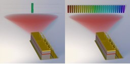
Figure 2: A high-end laboratory optical comb source vs a Pilot Photonics optical frequency comb source.
Optical comb lasers have a unique behaviour that can be exploited to provide next generation data transmission, next generation time and distance measurement, and next generation precision sensing. This unique capability is derived from the very precise spectrum of light that comb lasers emit, where each emitted frequency, or colour of light, is precisely locked to a controllable center frequency.
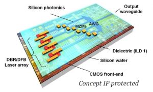
Photonic integration is a state-of-the-art semiconductor processing technique in which multiple photonic functions (the generation, modulation, amplification and detection of light), are integrated onto a single semiconductor chip. This drives efficiencies in cost, size, power consumption when compared to traditional techniques based on individual optical components (lasers, detectors, modulators, etc) attached together to carry out the same function.
Current optical transceiver products have a significant manual integration cost. The microchip revolution of the 1960s integrated multiple electronic components onto silicon chips. In the same way, photonic integration is revolutionising the photonics industry, and by 2022 photonic integrated circuit (PICs) will be widely adopted and beginning to replacing electronic ICs in certain applications .
Pilot Photonics’ founding team were among the first to use optical comb lasers for communication applications and developed patents in the area,. The company owns the patent rights to a type of optical comb generation known as gain switching which is highly suited to photonic integration. While most optical comb lasers have a fixed spacing between the frequencies, Pilot’s approach has the advantage that the spacing can be set precisely and swept quickly, allowing it to be used in a wider range of applications.
With the combination of its comb laser IP and its photonic integration capability, Pilot has developed the world’s smallest, and most versatile optical comb source.
Approach
For the same reason that computer processors rose in speed from the Pentium P5 (60MHz) in 1993, up to the Pentium D (3.76GHz) in 2006, before maxing out in speed and eventually having to switch to parallel multi-core processors, the optical communication industry must also transition to parallelism in its optical transmission systems to continue to progress, with single wavelength optical channels being replaced by multiwavelength “superchannels” [[i]].
Optical combs are the ideal laser technology to achieve this. Almost all of the highest capacity data transmissions ever recorded in R&D labs are based on optical frequency combs [[ii], [iii]], and despite the fact that the Optical Internetworking Forum (OIF) now include comb sources in their “Technology Options for 400G Implementation” [[iv]] no comb source technology suitable for use in long haul optical networks has been brought to market to date. There are two reasons for this:
- First, many of the commonly used techniques for the generation of optical frequency combs are bulky, unstable, or have poor optical performance (linewidth and relative intensity noise, or RIN).
- Second, techniques used for the separation of comb lines for modulation are based on optical filters that tend to be high loss and require optical amplifiers to compensate for this loss which adds cost, noise, complexity and bulk to the transceiver.
Pilot Photonics has developed a suite of Intellectual Property on optical combs that solves these problems and makes optical frequency combs attractive for use in optical network equipment for the first time. Both solutions are innovative by themselves, but combined together they offer the potential for truly disruptive innovation.
Capability 1: Stable Optical Frequency Comb Generation
The most commonly used approaches in the generation of optical combs for communications include mode-locking of semiconductor lasers (MLL) and the utilization of strongly driven electro-optic modulators (EOMs). While MLLs can generate wide spectral combs, the comb lines typically have large linewidth and low power, which make them unfavourable for use with high speed coherent optical modulation. MLLs also suffer from a complex fabrication process and a fixed free spectral range that is based on cavity length and therefore difficult to define precisely. The use of EOMs offers continuous FSR tunability but requires complex dual drive or cascaded modulators to obtain a broad and flat comb. Moreover, modulator properties such as bias drift and high insertion loss can prove problematic.
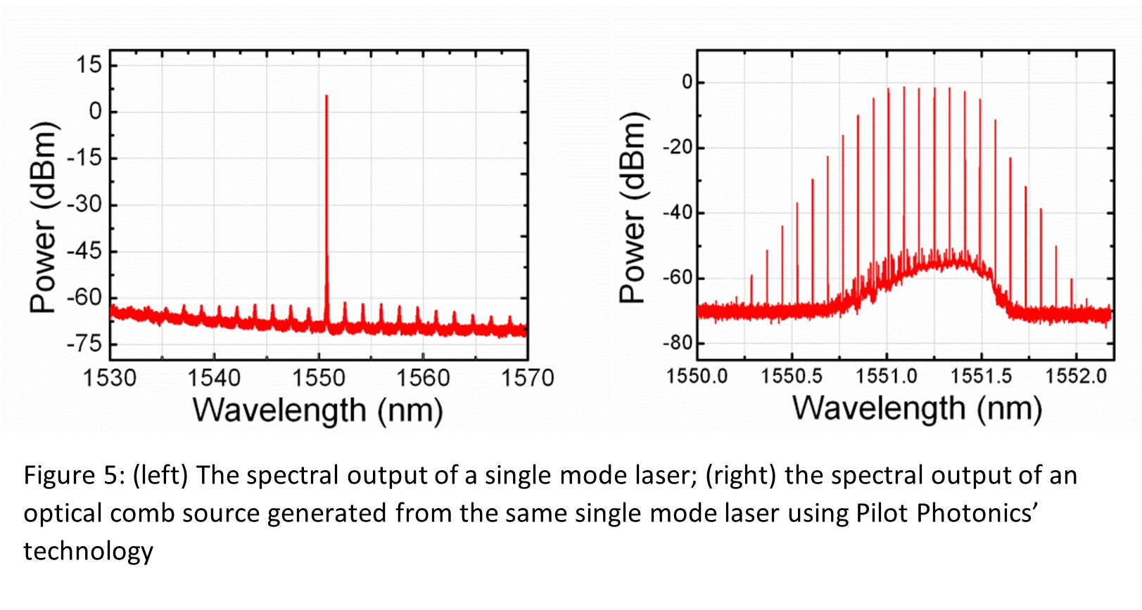
Based on two core patents [7, 8] Pilot Photonics produce optical frequency combs by gain switching an externally injected semiconductor laser diode in a technique that has proven to be simple, flexible and cost efficient. We have shown that this approach is ideal for photonic integration and tunability in wavelength and FSR (5 to 40 GHz) can be achieved. Furthermore, beneficial properties can be achieved from external optical injection, such as an improvement in the comb line stability and coherence, spectral flatness and transfer of the narrow linewidth of the master laser to the slave comb lines. In tests at Karlsruhe Institute of Technology, 1Tb/s and 2 Tb/s transmission superchannels was transmitted using Pilot Photonics comb sources.
Capability 2: Cost-effective Demultiplexing of comb lines
The second capability enabled by Pilot Photonics’ intellectual property is the cost-effective demultiplexing of the wavelengths for modulation. The conventional approach to the demultiplexing of optical frequency combs for modulation is to use an optical filter such as an Arrayed Waveguide Grating (AWG). The problem with this approach is that the suppression of adjacent wavelengths is difficult, particularly at narrow spacings and importantly, the filters tend to be lossy, necessitating the use of optical amplification inside the transceiver which adds bulk, cost and noise and leads to an inelegant solution. The patented PICOMB approach is based on the optical injection locking of an array of semiconductor lasers to provide simultaneous demultiplexing and noise free amplification of the wavelengths in what is effectively an active optical filter. The optical power from the injection locked laser array is sufficiently large to drive an array of modulators to encode high-order modulation formats on the frequency locked wavelengths.
Combining comb generation and demultiplexing in a single chip for truly disruptive innovation
The combination of these two capabilities has the potential to make optical comb sources suitable for use in coherent optical networks for the first time. The benefit and elegance of the solution is that both capabilities can be monolithically integrated into a single comb source & demux chip. Furthermore, the PIC comb source can be integrated with high-end data modulators further enhancing the value of the offering, and increasing its chances for commercial success.