- Component designs, fabrication and measurements
- packaging techniques and realization of sub-assemblies
- development of the III-V on silicon technology
- III-V to Si optical coupling
- first wafer run of III-V and silicon components with the novel developed integration technology
- III-V light sources and the electro-photonic integrated circuits (EPIC)
- techno-economic study of DIMENSION technology
- dissemination, exploitation and standardization activities
…for more information, please see reports on deliverables page and publications.
WP1 – Project management
The overall coordination and communication among the partners were continued and the project was finalized in September 2020. Further project meetings were organized and the mode of all-hands web conferences every three weeks was retained. In total the DIMENSION consortium met 10 times face to face and completed almost 70 web conferences. During the reported project period, 8 project deliverables and 4 milestones were achieved. Accordingly, deliverable reports have been prepared and submitted. The three recommendations received from the second review meeting were appropriately addressed. According to the technical challenges and delays in the second project period, a project amendment was organized and approved. This includes a project prolongation until September 2020, an update of the Description of Action (DoA) regarding the re-definition of objectives and demos as well as a re-organization of the work/time plan with tasks, deliverables and milestones. Furthermore, the consortium experienced a change, since the partner AIT terminated its contribution by November 2019. The remaining task and deliverable responsibility was transferred to IBM. Further challenges were brought to the project by the COVID-19 outbreak in the first half of 2020. Due to the lockdown in the participating European countries, all DIMENSION partners were affected by limited and reduced operability in the labs, clean rooms and workshops between March and June 2020. The delivery of required materials and components from different vendors was also delayed. Therefore, assemblies and measurements could not be continued as planned and also the further progress of the Run1 processing went on slower. However, in principle DIMENSION has made good progress in the third project phase. We were able to show the feasibility of the integration technology until the III-V integration on Si FEOL. Several Tx and Rx sub-assemblies have been built and the EPIC chips, i.e. the monolithic drivers and modulators as well as photodetectors and transimpedance amplifiers were successfully characterized. Correspondingly, further dissemination activities were performed. Finally, we were not able to finish all tasks due to the additional delays. For example, the BEOL processing of the III-V on Si and further measurements of EPIC chips are ongoing and planned to be finalized until the final Review Meeting. With the final deliverable reports and the final periodic project report all DIMENSION results will be summarized and the project activities will be completed. The planned and available resources were sufficient to perform all tasks and no changes were requited.
WP2 – System requirements, transceiver specifications and benefits evaluation
The work focused on the last task about the feasibility of the new integration technology, its implementation and evaluation including a cost study. Comparing different integration schemes with the DIMENSION technology reveal different prospects and challenges for the technical functionality potential. Today, the ‘hybrid integration’ and the ‘integrated III-V on Si’ platforms obtain tremendous traction in the market. However, the trend to larger interconnect bandwidth and the urgent need to improve power efficiency drive towards solutions with tighter electro-optical integration. This holds at system, sub-system and device-level. One can state that the ‘CMOS embedded III-V on Si’ platform, as developed in DIMENSION, offers the best performance and simplest form factor. Currently, companies like GlobalFoundries and Sicoya offer SiP platforms with monolithically integrated (Bi)CMOS functions. The success of these platforms will be important for the DIMENSION technology to find a path to market. The additional integration of active optical functions onto these platforms is a logical next step towards increasing the functionality. The co-integration of (Bi)CMOS functions in established ‘Integrated III-V on Si’ platform could also be feasible but will require a larger research and development effort. Furthermore, the market potential is highly dominated by the system-level cost of the underlying technology. Certainly, the monolithic integration approach targeted in DIMENSION is expected to have lower costs compared to hybrid solutions. The cost reduction will be associated mainly with the production of the chip, but will also drive down the costs of packaging and testing that are the prevailing ones in current implementations. Our analysis shows that by applying the DIMENSION technology, the transmitter cost will be at ~40 % of today’s cost with hybrid integration approach. Considering further innovations and optimization of the technology towards higher yield and volumes the transmitter costs decreases to 10% by 2030, which is still less than the costs with discrete technology (expected to be ~30% of today).
WP3 – Optical component design and fabrication
The development of III-V lasers and further processing of III-V on Si continued. The different approaches for current injection, i.e. lateral (LCI) and vertical current injection (VCI), were further investigated. While VCI suffers from high losses and it is challenging to show CW lasing at room temperatures, LCI is the best candidate for directly modulated lasers. However, LCI is more difficult to fabricate and by now, it was only possible to show luminescence but no lasing. Instead, high-speed integrated photodetectors with >70 GHz bandwidth and responsivities >0.5 A/W were demonstrated with LCI.
With the handover of the Si PIC and EPIC wafers from IHP, IBM started to process the III-V structures. Two technology demonstrators, each with two variants were defined: 1a) demonstration of III-V bonding on IHP SiP PIC with a reduced III-V to Si distance (300 nm) and without a back end of line (BEOL); 1b) demonstration of light coupling between Si and III-V material with thick gap (as in the EPIC stack) using a-Si waveguides; 2a) III-V integration on IHP EPIC technology with limited BEOL at IBM on chip-level to test if III-V process is compatible with electronics and SiP; 2b) full process of III-V integration on EPIC technology with BEOL demonstrating III-V functionality (LED) and electrical functionality (current mirror) on one chip. With demo 1a, it was possible to show the successful bonding of the III-V on the Si wafer. With demo 2b it was possible to verify the optical coupling from III-V to Si by using amorphous-Si (a-Si) waveguides with Si to a-Si coupling loss of 0.2-0.5 dB. With demo 2a, the successful integration of LEDs on EPIC wafers was shown. Electrical and electro-optical LED measurements have proven the principle functionality. However, LED currents much lower than expected have been observed and the light emission was observed at rather high voltages, which has to be further investigated. Finally, the III-V processed wafers were handed over to IHP for the Si BEOL processing towards demo 2b. Next to the bonding of the III-V structures on Si wafers, also the direct growth of III-V gain stack on a SiP platform for the main building blocks of the III-V on Si integrated laser was further investigated. We demonstrated that crystalline Indium Phosphide on Insulator crystals can be obtained by direct growth on Si, using an epitaxial growth technique in empty oxide cavities. Such InP crystals can serve as micro-substrates for the overgrowth of optically-active quantum-well structures. Finally, it was possible to successfully characterize of optically-pumped lasers on microscale devices at room temperature.
WP4 – Electronic design and electro-optic integration
The WP focused on both, the continued design and measurement of integrated driver circuits and electro-optical devices, and on the further processing of the III-V on Si devices with progressing Run1. To proceed with the III-V on Si testfield for the co-integration of driver electronics, SiP modulators and active III-V light sources, several technological requirements have been resolved: i) sufficient wafer planarization for the wafer bonding; ii) optical III-V to Si coupling (as mentioned in WP3), where we refrained from using poly-Si adiabatic couplers and rather used the coupling via a-Si waveguides, and iii) contamination test to handle the wafers between IHP and IBM in order to enable subsequent BEOL processes in IHP cleanroom. After handing the Si wafers over to IBM, the III-V structures where processed before transferring them back to IHP for the BEOL processing, which is still in progress. Due to the clean room delays caused be the COVID-19 lockdown, this can just be finished after the project finalization. Regarding the IC and EPIC design, further components have been realized, including a PAM-4 MZM driver with breakdown voltage doubler (BVD) for 100 Gb/s with 7.2 Vppd output swing, and a high-speed linear BVD modulator driver with a bandwidth of 78 GHz for a data rate of >100 Gb/s, with a THD <1%, a gain of 15.4 dB and an output voltage swing of 7.6 Vppd at a power consumption of only 740 mW. Furthermore, a co-integrated photodetector and transimpedance amplifier (PD-TIA) have been successfully designed and measured in EPIC technology for 50 Gb/s with 1.6 pJ/bit and a sensitivity of -3.7 dB (OMA) at a transimpedance gain of 70 dBOhm. In total, almost 20 drivers and EPIC designs have been realized during the entire project. Most of the components have been intensively measured electrically and electro-optically. However, some of the components still have to be characterized due to the lab down time due to COVID-19 lockdown.
WP5 – Packaging and characterization and evaluation of demonstrators
Different setups and approaches for component assembling and characterizations were verified. With respect to measurements on sub-assemblies and systems, the packaging techniques for electrical and optical coupling have been further investigated. With the verification of the wire-bonding process, it revealed that the used Au ball bonding is advantageous over alternative Al wedge bonding. The focus on the optical coupling has been on the connection of the optical fiber to the grating couplers of the EPIC chips. An optimized hexapod alignment procedure has been developed to achieve minimum coupling losses. Primarily FVA attach has been used for the coupling. For this, a special gripper has been designed and fabricated for the attach. Finally, several test PCBs have been realized for the Tx and Rx EPIC chips. Multiple assemblies have been built. As an outlook to the system integration of DIMENSION’s III-V on Si chips, an overall system integration packaging concept was developed, which features small footprints, low profile FVA attach and flip-chip bonding. For the measurements different methods have been further investigated for the application in the final validations. These include for example optical probing with fiber arrays and horizontal coupling. Finally, intensive electro-optical measurements and system experiments of the EIPC chips have been successfully performed with good results.
WP6 – Dissemination, Exploitation and Standardization
Further activities have been followed also in the third period of the project including for example further scientific publications and continuous update of the webpage with visitor statistics. To secure the rights of DIMENSION’s key findings, multiple patent applications have been granted and are available for licensing to third parties. In total, the project achieved more than 50 scientific publications and conference introductions, including seven journal papers and 4 Best Paper Awards, and a huge number of press releases and media coverages. Two workshops have been organized during the project duration enabling fruitful exchange of knowledge and experience. With their work on the project already three PhD students achieved their PhD and one postdoc achieved his state doctorate. Three further PhD students are approaching their degree. The consortium also extended the activities in standardization for IM/DD and coherent data transmission by considering the new JEDEC SiP group next to COBO, CohOBO and IC-TROSA, IEEE 802.3bs (400G Ethernet). Therefore, the project is well aligned to industry standards and ahead of the curve in some instances. Another interesting opportunity of the DIMENSION techniques could also be in co-packaged optics. Finally, the project partners identified project results ready for exploitation.
Driven by the demand of higher bandwidth density in data center interconnect systems, optical switches and other interconnects, the evolution of various past, present and future form factor standards for optical transceivers shows irrespective of the specific application a clear trend towards smaller footprint, lower power consumption and higher optical performance. Figure 1 (Source: https://ethernetalliance.org/ea/) shows a selection of form factor pluggables.
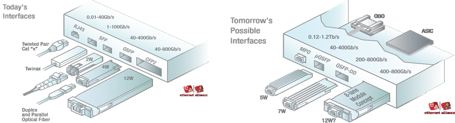
To satisfy these demands and to enable smaller optical engines, photonic integrations lends itself as a potential solution. As observed in the world of electronics, where closer and closer integration offered huge benefits in all the important metrics, the same level of gain is expected from photonic integration. Certainly, we have seen in the very recent past an uptake of photonic integrated circuits (PICs) in the market [https://www.lightcounting.com/]. However, despite early promises to enable large volumes of PICs at a low cost, the PIC market is driven by high-end devices. One might cite several reason, why that is the case, however, one major factor is the high initial cost associated with PICs: Up to 80% of cost in optical subassemblies is related to packaging, as no real standards – as e.g. for electronic ICs – are available to optical packaging. A second significant cost driver is related to the choice of materials in PICs: Certainly, for absolute lowest cost the preferred material is silicon. The availability of mature fabrication processes from the electronic IC industries, which produces enormous quantities of dies at remarkable yields, also allows for high volume and low cost manufacturing of photonic dies. However, the intrinsic properties of silicon (the indirect bandgap at telecom wavelength result in a quantum efficiency of around 10^-6) prevent it from efficiently emitting light. Light-emitting capabilities, however, are the major advantage of InP, a compound III-V semiconductor, which produces light very effectively at both important wavelength windows of 1.3 µm and 1.55 µm. Admittedly though, InP does not profit from mature manufacturing processes as seen in the silicon industry and is therefore more costly on a wafer and die level. Due to less reliable processes, which result in lower yields, smaller wafer sizes available and the need for more expensive hermetic packages, InP dies are generally more expensive than their silicon counterparts.
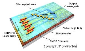
The DIMENSION projects aims to address all these challenges by combining the best properties of silicon with the light-emitting capabilities of InP. By integrating InP layers in the back-end of a CMOS compatible silicon photonic line, the shortcomings of silicon will be overcome and all functionality that is needed for an optical transceiver System on a Chip (SoC) will be made available on a single platform. Having electronic ICs, passive photonic ICs and active light sources on a single chip enables truly compact optical transceivers that easily fit any of today’s form factors and will ultimately result very high density optical transmission systems.
An application example is the Integrated Coherent Transmit Receive Optical Sub-Assembly (IC-TROSA) shown in Figure 2.
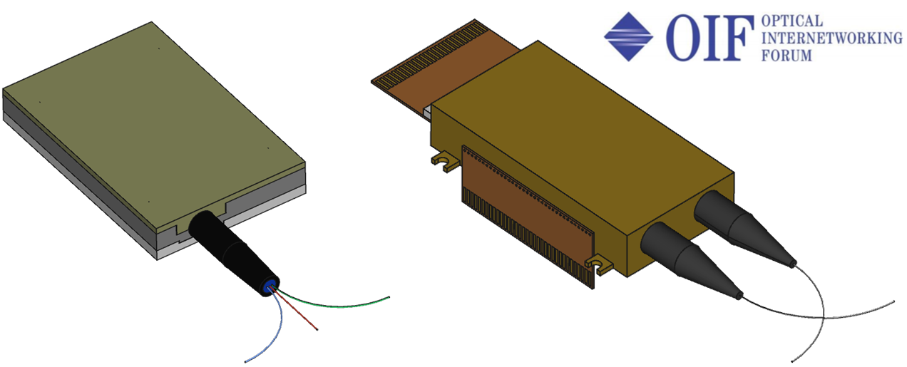
The OIF projects defines two variants of a board-mountable optical engine (BOE) for the use in coherent applications. The small footprint of both packages require photonic integration. Variant a (Figure 2, left) shows a non-hermetic package with a BGA connector on the bottom side aimed at silicon photonic applications, while variant b (Figure 2, right) is a hermetic package to be used with InP PIC and integrated laser source. Even though variant b is much larger compared to variant a, it is expected to feature a much lower level of integration as hermetic packages require much more space. Variant a, however, relies on an external laser, which is fiber coupled to the IC-TROSA and thus still requires additional space on the host PCB in addition to fiber routing in between. Applying the DIMENSION technology to this concept would allow vendors to build an IC-TROSA that exhibits all the benefits of variant a – BGA mounting, non-hermiticity, small footprint and a high level of integration, while additionally integrating a laser source without the need for additional external components and fiber routing. Such a device would easily enable very small form factor pluggables such as COBO, OSFP and even QSFP-DD to be used in coherent applications and thus significantly increase bandwidth density of data center interconnects and other similar applications. The added bonus of significant cost reduction together with higher bandwidth available to cloud based enterprises, ISPs and other businesses, is desperately needed to ensure tomorrow’s bandwidth intense applications and services can be provided to the end user.